Printed Circuit Boards (PCBs) are the beating heart of modern electronic devices, serving as the foundation for connecting electronic components. Whether you are building a simple hobby project or a complex consumer product, understanding PCB design is crucial and places you at the forefront of the dynamic evolution of electronics. This guide will cover the principles of PCB design, techniques, tools, and best practices, ensuring your designs are efficient and effective and that you are part of this progressive field.
What Is PCB Design?
PCB design refers to creating the layout and functionality of a printed circuit board, which involves arranging electronic components and routing electrical connections to optimize space, performance, and reliability. A well-designed PCB facilitates effective electrical connections and ensures manufacturability and ease of assembly.
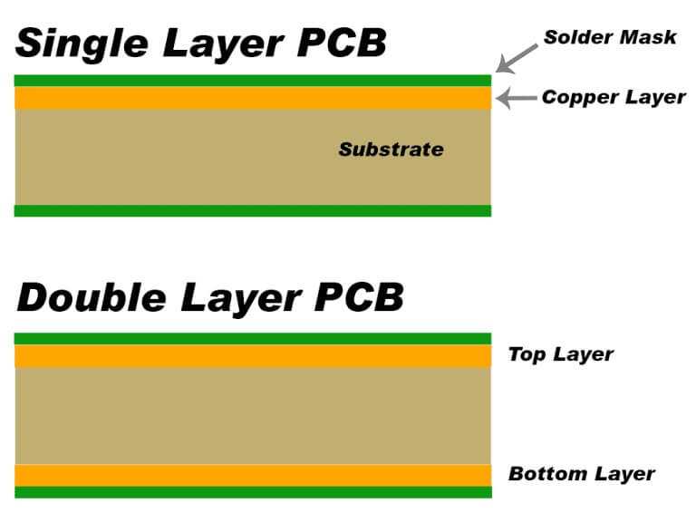
Key Components of PCB Design
Here are the fundamental components you will encounter in PCB design:

- Substrate: The base material, usually fiberglass or epoxy, supports the PCB.
- Copper Layer: Thin layers of copper that create pathways for electrical connections.
- Solder Mask: A protective layer to prevent solder from bridging between conductive paths.
- Silkscreen Layer: Printed markings on the PCB used to identify components and provide references for assembly.
Principles of Effective PCB Design
1. Define Your Requirements
Before starting the design process, define the following:
- Functionality: Determine what the PCB needs to accomplish.
- Size: Establish dimensions based on device constraints.
- Environmental Conditions: Consider factors like temperature, humidity, and exposure to elements.
2. Component Placement
Strategic placement of components enhances performance and simplifies assembly:
- Group Related Components: Place components with similar functions close together to minimize trace lengths.
- Avoid Crossovers: Ensure that sensitive traces are separated from power traces to reduce interference.
- Consider Thermal Management: Place heat-generating components in locations that allow efficient heat dissipation.
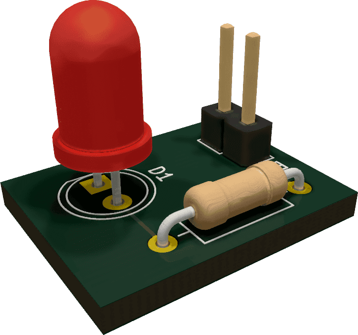
Example Layout
Here is a simplified layout of a PCB for an LED circuit:

3. Trace Routing
Routing involves designing the pathways that connect components:
- Width Matters: Use wider traces for high current paths to prevent overheating.
- Minimize Lengths: Keep traces short to reduce resistance and potential interference.
- Via Usage: Use plated-through holes (vias) sparingly; each via adds inductance and resistance.
Trace Width Calculation
The width of traces, which are the conductive paths on the PCB, can be determined using online calculators or formulas. For example, for a 1A current with a temperature rise limit of 10°C, you can use the following formula to calculate the trace width:
W=(ΔTI)β
Where:
- ( W ) is the trace width in mils.
- ( I ) is the current in amps.
- ( ΔT ) is the temperature rise.
- ( β ) is a constant based on the PCB thickness.
Using a PCB with a copper thickness of 1 oz/ft². We will use the values provided:
Given:
- Current ( I ) = 1 A
- Temperature rise limit ( ΔT ) = 10°C
- ( β ) for 1 oz copper is typically around 0.44.
Now, substituting these values into the formula:
W=(ΔTI)β
Substituting the values:
W=(101)0.44
Calculating (101):
- (0.10.44≈0.3981)
Now, since ( W ) is in mils, we need to multiply this by 1000 to convert to mils:
W≈0.3981×1000≈398.1 mils
Thus, for a 1A current with a temperature rise limit of 10°C on a 1 oz copper PCB, the trace width ( W ) will be approximately 398.1 mils.
This width ensures that the PCB can handle the specified current without exceeding the temperature rise limit, thereby maintaining safety and reliability in the circuit design. Adjustments to ( I ) or ( ΔT ) will affect the trace width needed for different scenarios.
4. Design Rules and Clearances
Adhere to manufacturer-specifics regarding spacing and component placement to avoid issues during production. Design rules include:
- Minimum Trace Width: Typically 10 mils for general applications.
- Clearances: Maintain adequate spacing between traces and components to prevent shorts or crosstalk.
Selecting the best tools is crucial for efficient PCB design. Here are a few popular software options with links to their respective websites:
- EAGLE: A user-friendly software that is excellent for beginners and pros alike.
- KiCad: Open-source software with extensive features ideal for advanced users.
- Altium Designer: This tool offers robust tools for complex designs and is frequently used in professional settings.
- EasyEDA: A web-based design tool great for quick prototyping solutions.
Best Practices for PCB Design
1. Prototype and Test
Always create prototypes and conduct tests to validate your designs before full-scale production. This step allows you to:
- Identify errors or design flaws early.
- Iterate quickly based on feedback.
2. Documentation
Documenting your design process, including schematics, layouts, and changes made over time, is not just a best practice but a necessity. Comprehensive documentation ensures you are organized and prepared, aiding in:
- Collaborating with team members.
- Ensuring maintainability and scalability of designs.
3. Stay Updated
The field of PCB design is continually evolving. Stay informed about:
- New materials and technologies.
- Industry standards and regulations.
- Emerging design practices.
Conclusion
PCB design is a critical part of electronics engineering, requiring a blend of technical knowledge, creativity, and attention to detail. By following the principles outlined in this guide, utilizing the best tools, and adhering to best practices, you can develop high-quality PCBs that meet the demands of modern electronics. Whether you're a hobbyist or a professional, mastering these skills will enhance your ability to bring your electronic projects to life.
Credits

