
Transistors Explained: BJTs, MOSFETs & IGBTs with Real Part Comparisons
- Admin: IDAR Mohamed
- 13 Jun 2026
- 0
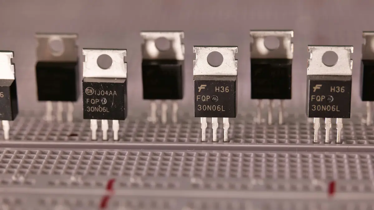
Every circuit board has transistors in it. The part numbers change, the package shrinks from TO-3 to SOT-23, but the job is the same: switch something on and off, or amplify a weak signal. What changes dramatically between circuit types is which transistor family makes sense.
Figure: Transistor packages have become dramatically smaller over time, from large TO-3 metal power packages to compact SOT-23 surface-mount devices used in modern electronics.
This guide covers BJTs, MOSFETs, and IGBTs with real part numbers, worked example calculations, and a selection table for common applications.
Table of Contents
- What Is a Transistor?
- Transistor Operating Regions Explained
- BJT vs MOSFET vs IGBT
- Common BJT transistors
- MOSFETs explained
- What is an IGBT?
- Darlington arrays: ULN2003A and ULN2803A
- Selecting the right device
- FAQs
What Is a Transistor?
A transistor is a three-terminal semiconductor device that amplifies a signal or acts as a controlled switch. In most modern circuits, it's the second role that matters: switching loads on and off, controlling motor speed, or routing logic signals.
Three major families cover most applications. BJTs (Bipolar Junction Transistors) are current-controlled. MOSFETs (Metal-Oxide-Semiconductor Field-Effect Transistors) are voltage-controlled. IGBTs (Insulated Gate Bipolar Transistors) are a hybrid type built for high-voltage work.
Each targets a different operating point. Choosing the wrong one adds heat, gate drive complexity, or efficiency problems.
Transistor Operating Regions Explained
Bipolar Junction Transistors (BJTs) operate in three primary regions, each dictating the transistor's behavior and application within a circuit: the Cutoff Region, the Active Region, and the Saturation Region. Understanding these regions is crucial for designing circuits that utilize transistors effectively as switches or amplifiers.
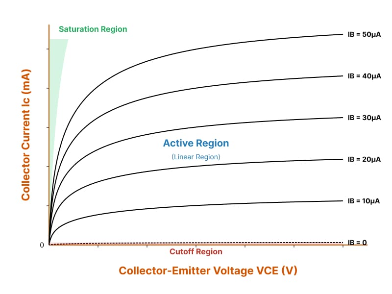
Figure: Collector current (IC) versus collector-emitter voltage (VCE) showing transistor cutoff, active, and saturation regions for increasing base currents (IB).
Cutoff Region
In the cutoff region, the transistor acts like an open switch. Both the emitter-base junction and the collector-base junction are reverse-biased. For an NPN transistor, this means the base current () is zero or very close to zero. Consequently, there is no significant collector current (), and the transistor effectively blocks the flow of current between the collector and emitter. This state is ideal for turning off a load or preventing signal flow.
Active Region
The active region is where the transistor functions as an amplifier. In this region, the emitter-base junction is forward-biased, and the collector-base junction is reverse-biased. A small change in the base current () leads to a proportionally larger change in the collector current (). This amplification is governed by the transistor's current gain, beta (β or ), where . The output characteristics graph for the Common-Emitter configuration clearly illustrates this, showing distinct curves for different values, where increases with up to a certain point and then flattens out, indicating a controlled current source. This linear relationship makes the active region suitable for analog amplification applications.
Saturation Region
When the transistor is in the saturation region, it behaves like a closed switch. Both the emitter-base junction and the collector-base junction are forward-biased. This occurs when a sufficiently large base current () is applied, causing the collector current () to reach its maximum possible value, limited by the external circuit components (e.g., collector resistor). In this state, the voltage across the collector-emitter () is very small, typically around 0.2V for silicon transistors, indicating that the transistor is fully turned on. The saturation region is critical for digital switching applications where the transistor needs to fully conduct current.
BJT vs MOSFET vs IGBT
| Parameter | BJT | MOSFET | IGBT |
|---|---|---|---|
| Control type | Current (base) | Voltage (gate) | Voltage (gate) |
| Drive requirement | Resistor + base current | Gate resistor only | Gate resistor only |
| Switching speed | Moderate | Very fast | Moderate |
| Voltage range | Up to ~200V typical | Up to 1000V+ | 600V to 6500V |
| On-state loss | |||
| Best fit | Amplifiers, low-freq switching | Power switching, motor drives | High-voltage inverters |
Below 100V at moderate-to-high frequencies, MOSFETs are the default. Above 400 to 600V, IGBTs often deliver better efficiency per dollar. BJTs remain useful for analog amplifiers and simple low-frequency switching.
Common BJT transistors
BC547 — General-purpose NPN
Rated at 45V and 100mA in TO-92. Standard for relay driving, LED switching, and interfacing microcontroller GPIOs to 12V loads.
Worked example: driving a 12V relay from a 3.3V GPIO
- Relay coil: 12V, 70mA
- Required base current:
- With 10x saturation margin:
The BC547 handles this with headroom. Above 100mA, move to the 2N2222 or 2N3904.
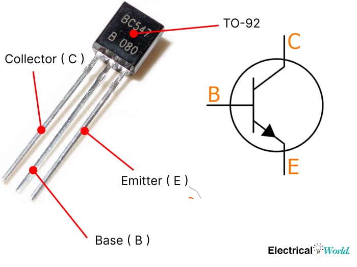
Figure: BC547 general-purpose NPN transistor in TO-92 package with collector (C), base (B), and emitter (E) pin identification.
2N2222 / 2N2222A — Classic NPN switch
Rated at 40V and 600mA, the 2N2222A is available in TO-18 and TO-92 packages. Compared to earlier variants, it offers a higher guaranteed current gain (), typically a minimum of 100 instead of 75 at 150mA, along with tighter manufacturing tolerances.
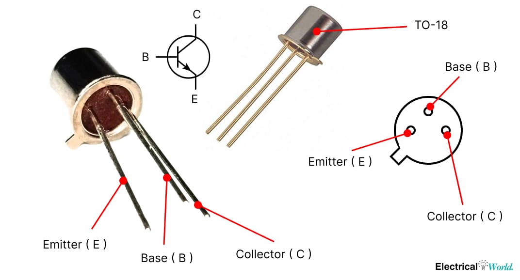
Figure: 2N2222A NPN transistor with collector, base, and emitter terminals labeled for circuit design and troubleshooting.
The actual can vary widely—from around 75 up to 300—depending on collector current and operating conditions. For reliable switching design, always base calculations on the minimum specification, not the typical value, to ensure proper saturation under worst-case conditions.
Example 1: Switching a Small DC Motor with a 2N2222A
A common use for the 2N2222A is driving small DC motors from a microcontroller. Since most GPIO pins can only source a few milliamps, the transistor acts as a switch that allows the motor to draw current directly from the power supply.
Components
- NPN transistor: 2N2222A
- DC motor: 6V, 150mA
- Base resistor: calculated
- Flyback diode: 1N4007
- Microcontroller GPIO: 5V
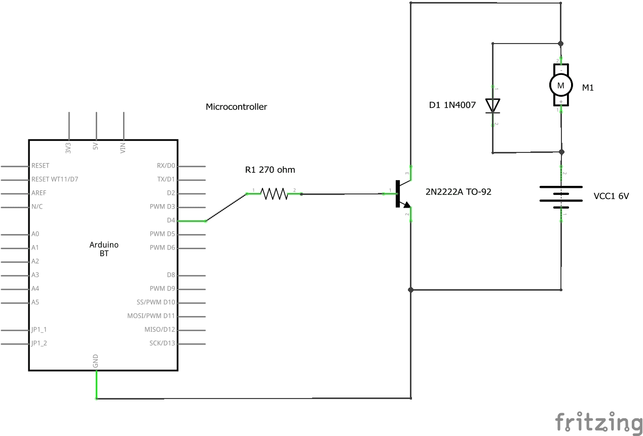
Figure: Typical 2N2222A transistor motor driver circuit showing a microcontroller GPIO controlling a 6V DC motor through a base resistor and flyback protection diode.
Step 1: Motor current
Motor running current:
Small DC motors can draw several times their rated current at startup, so it is good practice to leave additional design margin.
Step 2: Calculate required base current
For switching applications, the transistor should operate in saturation.
Instead of using the typical transistor gain, a forced gain of 10 is commonly used:
Step 3: Calculate the base resistor
GPIO voltage:
Base-emitter voltage:
Step 4: Choose a standard resistor value
The nearest standard value is:
This provides slightly more base current and helps guarantee saturation.
Step 5: Power dissipation in saturation
A saturated 2N2222A typically has:
Power dissipated by the transistor:
Only 30mW is converted into heat, so the transistor remains cool.
Flyback diode protection
When the motor is switched off, its winding generates a reverse voltage spike.
A 1N4007 diode connected across the motor terminals safely absorbs this energy and protects the transistor from damage.
Operation
- GPIO HIGH → transistor saturates → motor runs
- GPIO LOW → transistor turns off → motor stops
- Flyback diode suppresses inductive voltage spikes
Insights
The 2N2222A can easily switch small motors, relays, buzzers, and solenoids. By forcing the transistor into saturation, voltage drop and power dissipation remain low, improving efficiency and reliability.
2N3904 / MMBT3904 — Low-noise NPN
Rated 40V, 200mA. The 2N3904 is TO-92 through-hole; MMBT3904 is the SOT-23 SMD equivalent on the same die. The noise figure is slightly better than that of the 2N2222, so it tends to be the default for audio pre-amplifier stages and sensor interfaces where the noise floor matters.
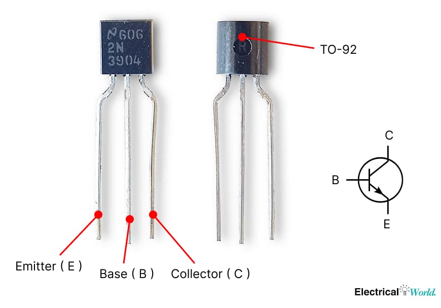
Figure: 2N3904 transistor pinout showing emitter, base, and collector connections used in signal amplification circuits.
2N3055 — Power NPN
60V, 15A, TO-3. The 2N3055 was widely used as a pass transistor in linear power supplies, where it regulates output voltage by operating in its linear region. It also appeared in audio amplifiers and early motor control circuits before MOSFETs became the standard for efficient switching applications. While modern designs prefer MOSFETs for switching, the 2N3055 is still useful in simple linear regulators where circuit simplicity matters more than efficiency.
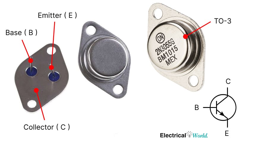
Figure: 2N3055 power NPN transistor in a TO-3 package. The case acts as the collector terminal.
MOSFETs explained
A MOSFET controls drain current with gate voltage. No gate current flows in steady state because the gate is capacitive. That's the key practical difference from a BJT: no continuous base current to manage. Gate drive circuits are simpler as a result.
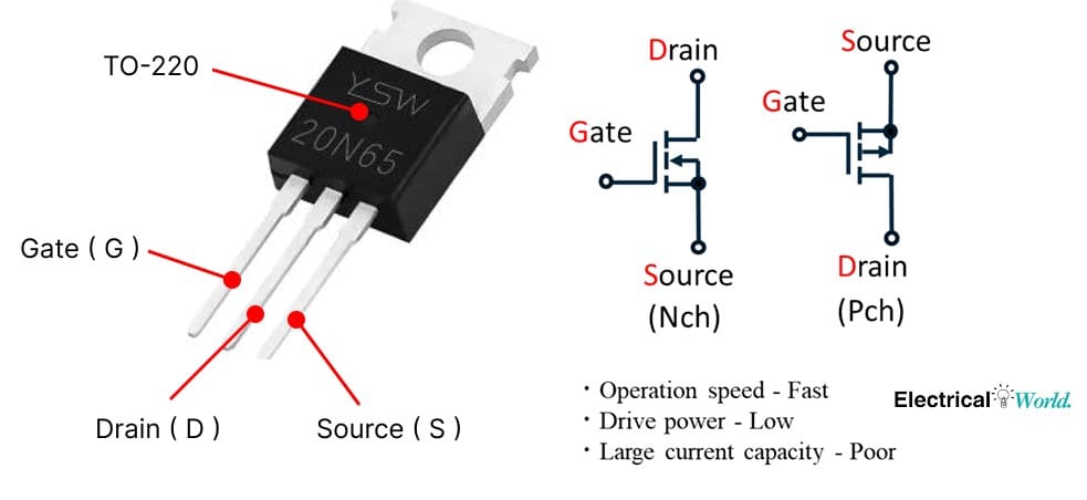
Figure: N-channel MOSFET structure and pinout. The insulated gate controls current flow between the drain and source without requiring continuous gate current.
For N-channel MOSFETs, the device turns on when exceeds the threshold voltage, typically 2 to 4V for standard parts and 1 to 2V for logic-level types.
IRFZ44N — Workhorse MOSFET
Specs: 55V, 49A, = 17.5mΩ at = 10V, TO-220.
Conduction loss at 10A continuous:
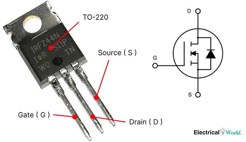
Figure: IRFZ44N MOSFET in TO-220 package with gate (G), drain (D), and source (S) terminal identification.
A small heatsink covers that. The IRFZ44N is common in PWM motor control, DC-DC switching stages, and low-side switching up to 55V.
Example 2: PWM Speed Control of a DC Motor Using IRFZ44N
MOSFETs are ideal for motor control because they require almost no steady-state gate current and have very low on-resistance.
Components
- N-channel MOSFET: IRFZ44N
- DC motor: 12V, 3A
- Gate resistor: 100Ω
- Pull-down resistor: 10kΩ
- Flyback diode: 1N5819 or 1N4007
- PWM source: Arduino / ESP32
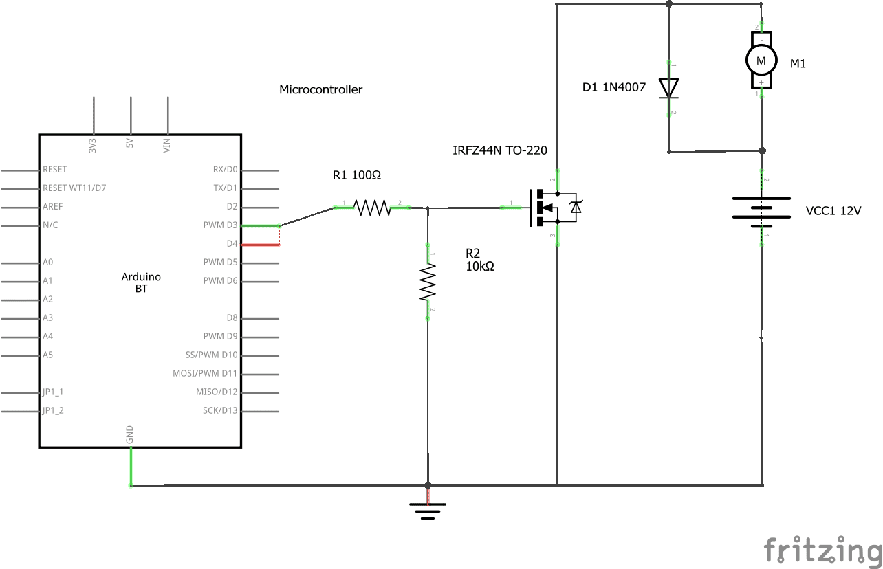
Figure: Components required for a PWM motor speed controller using an IRFZ44N N-channel MOSFET, a 12V DC motor, gate resistor, pull-down resistor, flyback diode, and a microcontroller PWM signal.
Step 1: Motor current
Motor rated current:
Step 2: MOSFET conduction loss
From datasheet:
Step 3: Gate drive condition
IRFZ44N is NOT fully enhanced at 3.3V logic.
So:
- Best case: use 10V gate drive
- Or use a logic-level MOSFET for 3.3V systems
Step 4: Gate resistor purpose
Gate resistor = 100Ω
Purpose:
- limits inrush gate current
- prevents ringing and oscillation
Gate current only exists during switching:
Step 5: Pull-down resistor
10kΩ ensures:
- MOSFET stays OFF during reset
- prevents floating gate behavior
Operation
- PWM HIGH → MOSFET ON → motor spins
- PWM duty cycle controls speed
- PWM LOW → MOSFET OFF
Insights
Unlike BJTs, MOSFETs do not require continuous input current. This makes them far more efficient for high-current switching applications like motors, LEDs, and power converters.
IRF3205 — High-current switching
Specs: 55V, 110A, = 8mΩ, TO-220.
Conduction loss at 30A:
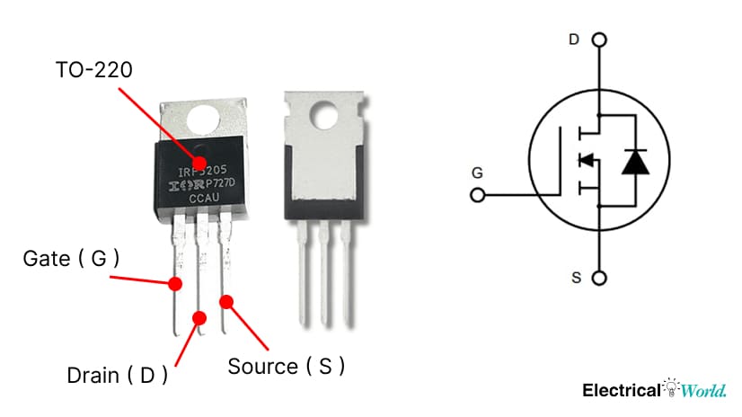
Figure: IRF3205 N-channel MOSFET showing gate, drain, and source pin assignments for high-current switching applications.
The lower on-resistance cuts conduction loss compared to the IRFZ44N at the same current. At 30A continuous, the IRF3205 needs a heatsink. It appears in battery management systems and high-current DC switches, where the IRFZ44N runs too warm.
2N7002 / 2N7000 — Small-signal MOSFETs
Rated 60V, 115mA (2N7002) and 200mA (2N7000), with threshold voltages below 2.5V. The 2N7002 is SOT-23; the 2N7000 is TO-92. Both turn on fully with 3.3 V or 5 V logic and appear in I²C level shifters, bus switching, and similar microcontroller-scale applications.
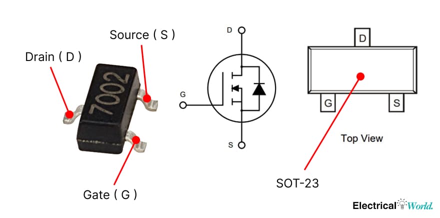
Figure: 2N7002 logic-level MOSFET in SOT-23 package with gate, drain, and source terminals identified.
What Is an IGBT?
An IGBT (Insulated Gate Bipolar Transistor) has a MOSFET-style gate and a BJT-style output stage: low gate drive current combined with high voltage capability and low saturation voltage at high currents.
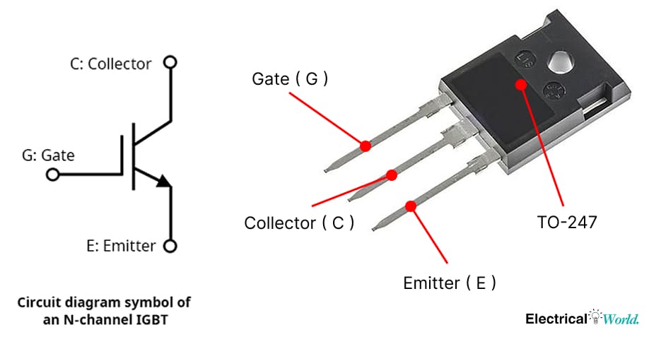
Figure: Typical industrial IGBT module with gate (G), collector (C), and emitter (E) power terminals identified.
Motor drives above 10kW use IGBTs. So do solar inverters above a few kilowatts, industrial UPS systems, and arc welding machines. The output stage of any VFD rated above 600V is almost certainly an IGBT module, not discrete MOSFETs.
The trade-off is switching frequency. IGBTs have a turn-off tail current that limits practical operation to around 20 to 50kHz. Above that, SiC MOSFETs are more efficient.
Darlington arrays: ULN2003A and ULN2803A
Driving multiple inductive loads from a microcontroller with individual transistors means individual base resistors, individual flyback diodes, and a cluttered PCB. The ULN2003A and ULN2803A consolidate this into one IC.
ULN2003A: 7 NPN Darlington pairs in DIP-16. Each channel is 50V, 500mA, with 2.7kΩ base resistors and flyback diodes already on the die. Compatible with 3.3V and 5V logic without external resistors.
ULN2803A: Same circuit, 8 channels. Use this when driving an 8-bit port or a relay bank mapped to a full byte of output data.
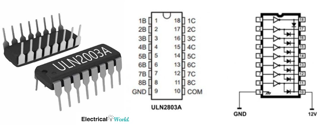
Figure: ULN2003A seven-channel Darlington driver IC with input, output, COM, and ground pin functions labeled.
Both devices are open-collector: the load connects between the output and the positive supply, and the IC sinks current on the output side. An Arduino driving 8 relays through a ULN2803A needs one IC, no external resistors, and no external flyback diodes.
BAT54S — Schottky clamp diode
The BAT54S is a dual Schottky diode in SOT-23. Not a transistor, but it consistently appears alongside MOSFET and BJT driver circuits for gate clamp protection, inductive flyback suppression, and supply OR-ing. Its 30V, 200mA rating and zero reverse recovery loss make it a compact, fast solution in transistor driver stages.
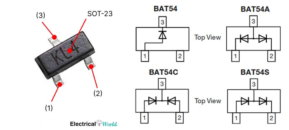
Figure: BAT54S dual Schottky diode package with pin numbering and internal diode connections.
Selecting the right device
| Application | Recommended Part |
|---|---|
| GPIO relay driver (12V, <100mA) | BC547 or 2N3904 |
| Multiple relay or motor bank | ULN2003A or ULN2803A |
| PWM motor control (<55V, <10A) | IRFZ44N |
| High-current DC switch (<55V, <30A) | IRF3205 |
| Logic-level signal switching | 2N7002 (SMD) or 2N7000 (DIP) |
| Linear regulator pass element | 2N3055 |
| VFD or solar inverter (>400V) | IGBT module |
| Gate clamp or flyback protection | BAT54S |
At higher currents, matters more than gate drive simplicity. The difference between 8mΩ and 17.5mΩ at 50A is 18W. At sustained duty cycles, that is real thermal load, not a rounding error.
Conclusion
Transistors may all perform the same basic function—controlling current—but the way they do it makes a huge difference in real-world circuits. BJTs remain useful for simple switching and analog amplification, MOSFETs dominate modern low- and medium-voltage power electronics thanks to their efficiency and fast switching, and IGBTs take over when voltage and power levels become too high for MOSFETs to remain economical.
The best choice is rarely the device with the highest current or voltage rating. Instead, it is the one whose characteristics match the application: a BC547 for a relay driver, a 2N7002 for logic-level switching, an IRF3205 for high-current DC control, or an IGBT module for industrial motor drives and inverters.
Understanding the trade-offs between drive requirements, switching speed, conduction losses, and operating voltage allows you to select the right transistor from the start—resulting in cooler, more reliable, and more efficient designs.
Related Posts
- PWM Motor Control: Complete Guide
- Variable Frequency Drive (VFD): Complete Guide
- Contactor vs Relay: Complete Guide
- PID Controller Explained
- Understanding Induction Motors
- Current Transformer Complete Guide: How CT Sensors Work, SCT-013 Wiring & Sizing
- Servo Motor vs Stepper Motor: Which One Actually Belongs in Your Build?
Helpful Calculators
- Ohm's Law Calculator
- AC DC Current Calculator
- Resistor Color Code Calculator
- Series Parallel Resistance Calculator
- Voltage Drop Calculator
- Power Factor Calculator
- Capacitor and Inductor Reactance Calculator
- Transformer Ratio Calculator
Credits
- Photo by Axel Richter on Unsplash
⭐ Was this article helpful?
IDAR Mohamed
Electrical Engineer
Electrical Engineer specialized in power systems, electrical installations, and energy efficiency. Passionate about simplifying complex electrical concepts into practical guides. (University of applied sciences graduate, with experience in HV/LV systems and industrial installations.)
- Semiconductors
- Electronics and Circuits


